


 |
|


| Robot Reference->Power Pack Schematics | |||
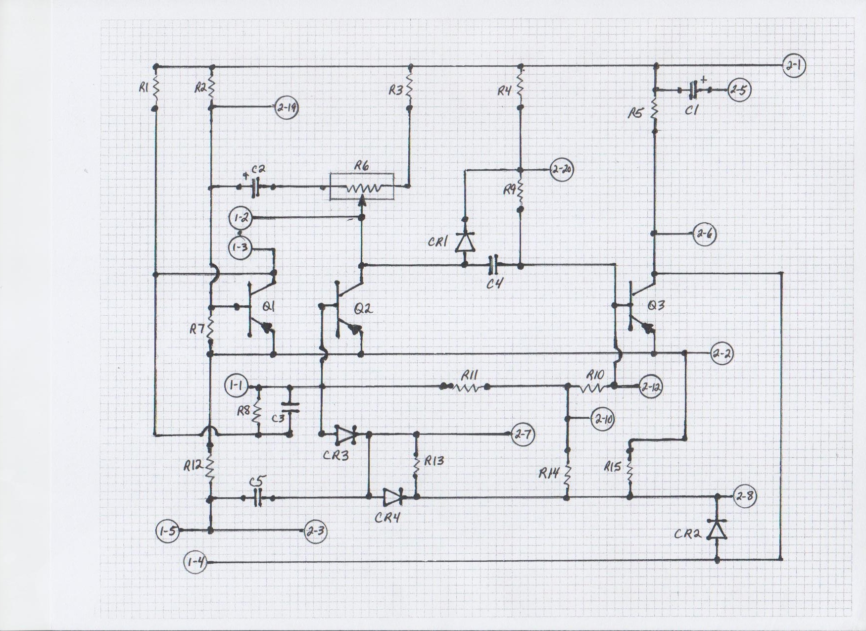
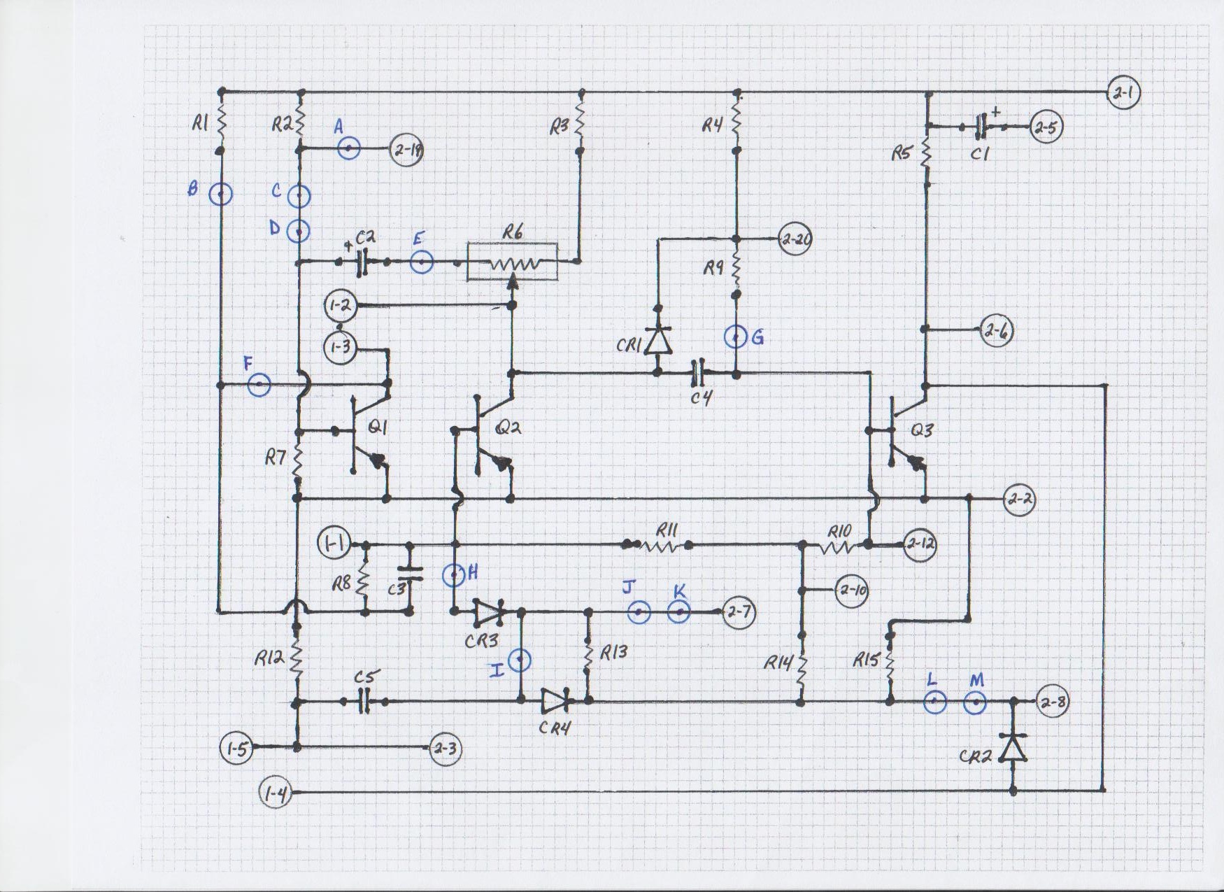
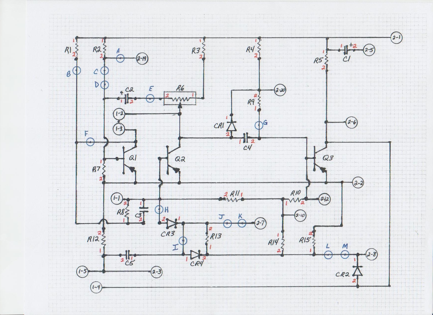
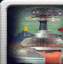
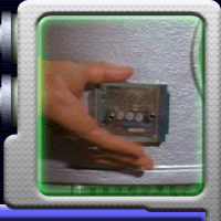
After joining the club and spending a long time trying to play catch-up to some of the basic knowledge of most of the other members, something began to get my attention. It was the power pack, and in particular, what did the actual circuit look like in a schematic. Granted, we don't need the schematic for anything whatsoever, but it just seemed like an interesting thing to know, especially since in a small way, it is sometimes used to complete the circuit for the power pack function of triggering the slump by its' removal. So, after many hours of evaluating the circuit board and many, many re-drawings of the slowly developing layout, all done by hand, a full circuit schematic began to develop. In the beginning, it was so easy to get confused tracing the circuits out, as the same component lead would often have very different connections on one side of the board than the other, I had to constantly be flipping the board over and the leads at the top were now at the bottom, or vice versa. Also, there were jumpers, also called Vias, that went from one side of the board to the other, and sometimes crossed back again. Add to this that I sometimes was interrupted for hours or days and had to try to find where I was before. The potential for confusion was huge, and I had to find out how to stop it as I chased out the circuit. I have traced out other circuits before to convert to schematics, but none before had this potential for confusion. Because of this, I had to develop some of my own simple circuit markings to help keep consistent as I keep going from one side of the board to the other. Identifying parts and leads comes in under the subject of "nomenclature", basically parts identification. But beyond the typical parts identification, I had to also identify the parts' leads, such as resistors and capacitors, and also even the jumpers. Some parts have a polarity, such as diodes, so they have their own lead identification, but for simplifying, all parts got their leads identified, as well as the two connectors, one at each end of the board. I will say this comment at this point. I will make the comparison of when I previously looked at sheet music. It meant absolutely nothing to me. Till one day when I was taught how to take a note viewed on the sheet music and press down the correct key on the piano. I now saw a relationship between the two. That day, a gap was bridged. Hopefully, in some way, the power pack that we use, that is so important to us, will take on a new perspective. Even as the Robot became Will's friend, the power pack will become less intimidating. There are three drawings of this schematic presented. Drawing #1 is the schematic with the components identified. Drawing #2 is the schematic with the components and board jumpers identified. Drawing #3 is the schematic with the components, jumpers, and leads identified. The following text helps explain the schematic information presented. As for the nomenclature, or parts and leads identification, here follows my explanation of their usage. I have tried to use basic and standard nomenclature as much as possible. There is a joke about liking standards so much, that this is why we have so many different ones. As you know, standards, by nature, eliminate variations. The point of this, is that some nomenclature has changed over the decades, even as parts have evolved. Unfortunately, even today, we sometimes have standards in this country, and different ones in Europe, so variations of standards still go on. During the time frame of this power pack, the more common transistors were germanium types, where today silicon is the material that most of made of, due to it's qualities. Also, a popular diode type back then was germanium. The diodes and transistors of this power pack are both of germanium construction. More common today, is to refer to diodes as "D" with a number, such as D1. During the time frame of this power pack, a common designation for diodes was "CR" such as CR1. There is discussion as to what the CR stands for, and two ideas are 1)current rectifier and 2)crystal rectifier. Two common rectifiers also around at this time were selenium and tube type rectifiers. Based on this, crystal rectifiers is probably the likely reference, as all basic diodes will limit current to one direction, so this wouldn't have been much of a clarification. In this schematic, the diodes will be referred to as CR1 to CR4, and as stated, they are germanium construction. As or transistors, they are also germanium and are referred to as Q1 to Q3. Also, they are PNP type transistors. If you want a challenge, try to find these as the actual transistors. To begin drawing this schematic, one task was to find out if the transistors were PNP or NPN. Fortunately I was able to find this information, so this helped in the accurate production of the schematic. As for the resistors, they are simple carbon composition resistors, and are designated as R1 to R5 and R7 to R15. They have no polarity and can be installed in either direction, but for attractiveness, are usually installed in a uniform manner, such as the main or starting color bands of the resistors facing the same direction. There is one part, R6, that is not a resistor, but rather a potentiometer, or variable resistor, sometimes used as a voltage divider. As for the capacitors, they vary in types and even used polarize parts. They are designated as C1 to C5, and polarity is identified when the part is polarized. There are two connectors used on the board. I refer to them as "1-" and a number for the five pin connector, such as 1-1 to 1-5 within a circle, and "2-" and a number for the 20 pin connector, such as 2-1 to 2-20 within a circle. I made an effort to put the connections for the five pin connector more on the left side of the schematic and the pins for the twenty pin connector more on the right side of the schematic. I didn't try to line them up in numerical order as this would have added much complication to the drawing, with many extra jumpers to get them into this order. A very subtle, but crucial part of the board are the jumpers, or Vias. These are the wiring connections passing from one side (top) of the board to the other (bottom). Normally, they will not have any designations of any type. In this effort to trace out this circuit, for me- the designations became a necessity. Since they are a connection, I showed them as a dot on the circuit path (wiring between parts), and enclosed this with a circle. To this, I added a capital letter of the alphabet, A to M. The addition of these nomenclature comments for the jumpers is mine and not a part of the circuit board. I do provide different schematic layout drawings, where different nomenclature is shown, as sometimes removing them adds to the clarity while viewing. My final identification usage is the identification of the leads of the parts. I used the numbers "1" and "2" for the lead identification, on each lead coming out of the component. I didn't use this on all the leads of the potentiometer, or on the transistor leads. Again, this is my designation, and not a part of the circuit board, nor is it a common thing to find on the schematic or parts list. It was just used to help keep track of the circuitry as I kept going back and forth to the top and bottom of the board, where different connections were made on the same component lead. These extra nomenclature identifications that I used, for lead identification and jumper identification, was tremendously helpful not only to complete the schematic, but also for verifying the relationship between the schematic and the original board when finished and trying to verify the accuracy. There were so many hours that I worked to develop this schematic and well over 150 redraws of this work, all done by hand. The frustrating thing in the redraws was that I would be 80-90 percent finished, I noticed how a different layout of the parts in the schematic would add to clarity, so I made notes and began a new redraw. I had several basic goals as I approached this work. One was accuracy, and another was clarity. The final layout needed to not look so confusing, even to a technician. I realized that most people viewing it would not be interested in it for its' technical information, but just to bridge that gap of technical intimidation. Even as I look at it now, the thought coming to my mind is how simple it looks, not at all like the power pack board. It looks so simple, it makes me wonder what then took so much time and effort. But with this, I realize that simplifying something, anything, and maintaining accuracy, is seldom an easy task. I will say that one of the most difficult things was HOW to begin this task. Where do you begin- at what part of the circuit? I decided to start by drawing the three transistors as individual circuits and then to piece them together and start adding other parts. After this, I began trying to straighten the mess up, a long process. Though I have traced out other circuits in the past, this one taught me some new things, at least in the area of methods. A key aspect of this schematic, is that this is a complete schematic of the power pack, including the parts usually removed for the addition of the three connectors that are used in plugging the power pack into the torso. There will be some other drawings forthcoming, including enlarged drawings of the circuit board where all these markings will be included to help show the relationship between the schematic and the circuit board. I am working with a very good friend, on these circuit board drawings, the top and bottom of the board, and will make sure that they show as much of the circuit as possible, even with the three connector mounting modifications, to mount to the torso. One thing that I have planned, is to make other modified power packs, one of which will be a surface mount component version, based on this schematic. Obviously, I will have to spread out the parts, or it will look pretty bunched up in the middle of the board, as they take so little space. It should make for a interesting "upgrade". In an effort to be nostalgic, since this is a 50+ year old device, I decided to present this as a hand drawn rendition, with graph paper on the background. I have worked so hard to try to make this accurate, holding back from presenting it till I checked it again and again. I have used a variety of sources from the internet and individuals, some of which I can't remember whose robot builds they came from. I can only say thanks to people who have helped and some whose pictures that they have posted, has been a tremendous help. In appreciation for the provisions that the information available has made this possible, I give my deep thanks. Thanks for the opportunity to present this, | |||
 Power Pack Schematics infomation